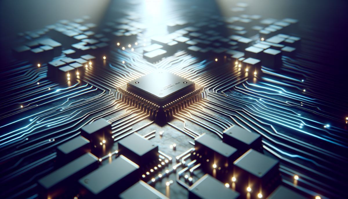
Moore's Law has always been less a law than a bet — a confident wager made by Intel co-founder Gordon Moore in 1965 that the number of transistors on a chip would double roughly every two years. For decades, the semiconductor industry honored that bet with remarkable discipline. But physics, as it tends to do, is now collecting its debts. Transistors have shrunk to the point where they measure just a few atoms across, and the thermal, electrical, and quantum-mechanical complications that arise at those scales are making further miniaturization increasingly expensive and increasingly marginal. The industry is not in crisis, but it is at an inflection point, and the response unfolding across chipmakers large and small is telling: artificial intelligence is being recruited not just as a product to be accelerated by chips, but as a tool to redesign the chips themselves.
The distinction matters more than it might first appear. For most of the past decade, the semiconductor conversation has centered on building faster, more efficient chips to run AI workloads. Now the feedback loop is closing. AI is being used to optimize chip architecture, simulate design trade-offs, and identify configurations that human engineers, working within the constraints of time and cognitive bandwidth, would never reach on their own. This is not a distant research ambition. It is already happening on the factory floor and in the design lab.
Samsung's approach illustrates one of the more consequential shifts in how engineers are rethinking the fundamental architecture of memory. Rather than shuttling data back and forth between memory and a separate processor — a process that consumes enormous energy and introduces latency — Samsung is embedding AI processing capability directly into its memory chips. The concept, known as processing-in-memory or PIM, treats the memory itself as a compute resource. The energy savings are significant because data movement is one of the most power-hungry operations in modern computing. For machine learning workloads in particular, where the same data is often accessed repeatedly during training and inference, eliminating that round-trip can produce speed and efficiency gains that no amount of transistor shrinkage could easily replicate.
This is a meaningful architectural departure, not an incremental improvement. It reflects a broader industry recognition that the bottleneck in AI computing is no longer raw processing power alone — it is the cost, in time and energy, of moving information. Samsung's bet is that the smarter move is to bring the computation to the data rather than the other way around. If that bet pays off at scale, it could reshape how data centers are built and how AI inference is priced, with downstream effects on everything from cloud computing costs to the energy consumption of large language models.
Google's fourth-generation Tensor Processing Unit offers a different but complementary lesson. The TPU V4 reportedly doubled the processing power of its predecessor, a gain achieved not through a generational leap in transistor density but through architectural refinement — better interconnects, smarter memory hierarchies, and design choices tuned specifically for the matrix multiplication operations that dominate neural network computation. Google has been designing its own AI chips since 2016, and the compounding returns of that investment are now visible. Each generation informs the next, and the design process itself is increasingly assisted by machine learning tools that can explore the vast space of possible chip configurations faster than any human team.
This is where the second-order consequences become genuinely interesting. As AI accelerates chip design, and better chips accelerate AI, the cycle tightens. The firms with the largest AI research operations gain the most from AI-assisted design, which produces better chips, which further extend their AI capabilities. The feedback loop is not neutral. It tends to concentrate advantage. Smaller chipmakers and national semiconductor programs that lack the data, the compute, and the engineering talent to participate in this loop may find themselves falling behind not linearly but exponentially.
The end of Moore's Law was supposed to be a leveling moment — a point at which the relentless pace of improvement slowed and the field opened up to new entrants with new ideas. Instead, the transition to AI-assisted design may be doing the opposite, handing the most resourced players a new compounding advantage just as the old one was expiring. Whether regulators, research institutions, or open-source hardware communities can interrupt that dynamic is one of the more consequential questions the semiconductor industry will face in the years ahead.
References
- Mack, C. (2011) — Fifty Years of Moore's Law
- Jouppi et al. (2023) — TPU v4: An Optically Reconfigurable Supercomputer for Machine Learning with Hardware Support for Embeddings
- Mutlu, O. et al. (2019) — Processing Data Where It Makes Sense: Enabling In-Memory Computation
- Waldrop, M. M. (2016) — The Chips Are Down for Moore's Law
Discussion (0)
Be the first to comment.
Leave a comment