The semiconductor industry has quietly shifted its center of gravity. For decades, the defining metric of chip progress was transistor density, the relentless march described by Moore's Law. But as that law has slowed to a crawl, a different kind of engineering has moved to the front: how you stack, connect, and package multiple chips together into a single, unified system. Intel, a company that spent most of the last decade watching rivals outmaneuver it on manufacturing, is now placing a very large bet that advanced packaging is where the next era of computing gets decided.
The timing is not accidental. The explosion of artificial intelligence workloads has created a demand for chips that can move enormous amounts of data between processors and memory at extraordinary speeds. Traditional chip design, where logic and memory sit on separate components connected by relatively slow pathways, has become a bottleneck. The answer the industry has converged on is tighter physical integration, stacking chips in three dimensions, connecting them with dense arrays of microscopic copper pillars, and shrinking the distance data has to travel to near zero. This is the domain of advanced packaging, and it is where Intel is staking a significant portion of its revival strategy.
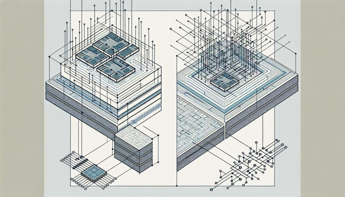
Intel's manufacturing division, Intel Foundry, has been pushing its Foveros and EMIB packaging technologies as core differentiators. Foveros allows chips to be stacked directly on top of one another, while EMIB, the Embedded Multi-die Interconnect Bridge, enables high-bandwidth connections between chips placed side by side. These are not incremental improvements. They represent a fundamental rethinking of what a chip actually is, moving from a single monolithic die to a mosaic of specialized tiles assembled with precision.
What is driving this urgency is the insatiable appetite of large language models and other AI systems for memory bandwidth and compute density. Nvidia's dominance in AI accelerators has been built partly on its ability to integrate high-bandwidth memory directly alongside its GPU dies, a packaging achievement as much as a silicon one. AMD has pursued similar strategies with its chiplet architecture. Intel, which pioneered some of the underlying packaging concepts, found itself in the uncomfortable position of having invented tools that competitors wielded more effectively.
The competitive pressure has forced a reckoning inside Intel. The company's decision to separate its product design and foundry operations into distinct business units was partly about accountability, but it was also about making Intel Foundry a credible option for outside customers who would never trust a competitor's internal chip shop. Advanced packaging capacity is central to that pitch. If Intel can offer external chipmakers access to Foveros or EMIB alongside its leading-edge transistor nodes, it becomes something more than a chip company. It becomes infrastructure.
There is a geopolitical dimension here that amplifies everything. The CHIPS and Science Act directed billions of dollars toward rebuilding domestic semiconductor manufacturing in the United States, and Intel has been one of the primary recipients of that federal attention. Advanced packaging facilities are explicitly part of what policymakers want onshore, because packaging is where final assembly happens, and assembly is a chokepoint that currently sits heavily in Asia. Intel building out domestic packaging capacity is therefore not just a business decision. It is entangled with national industrial policy in ways that give the company unusual political durability even when its financial results disappoint.
The deeper consequence worth watching is what happens to the broader ecosystem if Intel succeeds in establishing itself as a leading packaging foundry. Advanced packaging requires extremely close collaboration between chip designers and the packaging house, far closer than traditional foundry relationships. If Intel becomes a hub for that collaboration, it could pull design activity, tooling standards, and engineering talent into its orbit in ways that reshape who controls the architecture of future AI hardware.
There is also a feedback loop embedded in the strategy. As more AI compute gets built on advanced packaging platforms, the software frameworks and hardware abstractions that developers use will increasingly assume that architecture. That assumption, once baked into enough tools and models, becomes self-reinforcing. The company that sets the packaging standard early may find that the ecosystem does a significant portion of the competitive work for it.
Intel has been counted out before, and it has also disappointed before. But the convergence of AI demand, federal investment, and a genuine technical transition in how chips are built has handed the company a window that did not exist five years ago. Whether it can execute precisely enough, and quickly enough, to climb back through that window is the question the next several years will answer.
References
- Shilov, A. (2024) — Intel Foundry: Foveros and EMIB Packaging Technologies Explained
- CHIPS Program Office (2023) — CHIPS and Science Act Overview
- Cutress, I. (2023) — Intel Foveros Direct and the Future of 3D Packaging
- McKinsey Global Institute (2023) — Semiconductor Advanced Packaging: The Next Battleground
Discussion (0)
Be the first to comment.
Leave a comment